
SEMICONDUCTOR REVIEW THANK YOU FOR SUBSCRIBING
× 
Semi Conductor Review Weekly Brief
Be first to read the latest tech news, Industry Leader's Insights, and CIO interviews of medium and large enterprises exclusively from Semi Conductor Review
Semiconductor Review: Specials Magazine
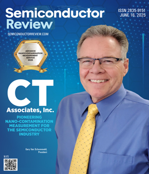
For more than three decades, CT Associates, Inc. has been at the forefront of contamination measurement, evolving alongside the semiconductor industry’s ever-increasing demand for precision and purity. What began as a focus on micro-contamination has shifted into nanoscale detection, where the tiniest particles—mere nanometers in size—can mean the difference between a flawless semiconductor wafer and costly defects impacting device yield. At the heart of CT Associates’ mission is a commitment to detect, measure and control contamination in liquids, a challenging area that demands technical expertise, innovative problem-solving and new method development. “Unlike conventional laboratory approaches that rely on extracting samples and analyzing them separately, we focus on a more dynamic route; measuring contamination in situ, directly within the operating equipment,” says Gary Van Schooneveld, President. “By doing so, we eliminate external contamination risks and achieve a level of accuracy that can improve detection by a factor of ten.” This approach has made CT Associates a trusted partner in the semiconductor space, where contamination control is critical. Rather than offering one-size-fits-all testing, the company collaborates closely with its clients to understand their specific challenges and designs customized tests and equipment that yield actionable insights—not just a set of lab results, but data that drive real-world solutions. Advancing Liquid Contamination Detection As integrated circuits shrink and transistor densities increase, the presence of even a single particle can compromise an entire wafer. The traditional understanding of contamination revolved around particles visible under optical inspection tools. But as technology progressed, the need for more advanced measurement techniques became apparent. With device design rules identifying killer particle sizes well below 10 nanometers, contamination has become a critical challenge. In the early days of contamination control, the industry was primarily focused on airborne particles as these were easier to detect, quantify and manage than in liquids. Cleanroom environments were designed to minimize particulate contamination, and air filtration systems were developed to ensure that semiconductor fabrication facilities maintained the highest standards of cleanliness. As progress was made in managing airborne contamination, contamination in liquids, including ultrapure water and high-purity chemicals used in semiconductor processing, emerged as significant sources of contamination. Unlike airborne particles, which could be effectively controlled with filtration and airflow management, liquid-phase contaminants were far more challenging to detect and mitigate. CT Associates pioneered methodologies focused on contamination measurement in liquids. This shift in focus proved revolutionary, providing semiconductor manufacturers with new insights into the sources of defects and yield loss. A breakthrough in this area was the ability to measure contamination in situ, meaning that samples did not have to be removed from the manufacturing environment for analysis. This eliminated the risk of external contamination and provided a much more accurate picture of the contamination levels within the production process.
Top Miniature and Ultra Miniature Transformers, Inductors, DC-DC Converters, And AC-DC Power Suppliers 2025
Pico Electronics was founded in 1967 by engineers Mr. Joseph Sweeney and Mr. Henry Spoldi, whose sole mission was to build the smallest, most reliable magnetic components on the market. Their commitment to setting the benchmark in miniaturization made their company the go-to aerospace and military magnetics and power supply manufacturer for applications that demand consistent high performance and durability under environmental stress. “Our forte is and always will be engineering compact and reliable electronic components for the most stringent applications,” says Fernando Da Rosa, electrical engineer. Its product portfolio features ultra-miniature transformers,inductors, and power modules which are available as DC-DC or AC-DC converters. Power ratings up to 150 Watts for transformers, 300 Watts for DC-DC converters and 2,000 Watts for AC-DC power modules are offered in various package configurations. With all standard products listed on the company website, customers are guaranteed an easy and seamless selection process. To better align the products with their application needs, clients can request modifications to existing components by initiating a request via phone call or email. Once Pico Electronics receives detailed specifications, it modifies the required component within a minimal lead time or develops a bespoke solution from scratch. Each product is engineered to comply with rigorous environmental and electrical standards to guarantee optimal performance when exposed to extreme temperature variations, intense vibrations and mechanical shocks. Many of its products are also featured in qualified product listings, signifying their adherence to military-grade reliability protocols. Pico Electronics’ quality assurance protocol necessitates implementing 100 percent vacuum impregnation for all transformers and inductors, unlike many manufacturers that limit this process to a few components. This proprietary method encapsulates the internal windings in a durable resin, significantly enhancing their resistance to moisture, chemical exposure and mechanical vibrations.

Electronics AI Design and Development Company of the Year 2025

At Think Circuits, science comes alive through the fusion of innovative engineering and visionary thinking. The company transforms ambitious concepts into intelligent, adaptive systems, redefining the role of hardware and embodied intelligence in today’s world. Rather than focusing solely on automation, Think Circuits leads the shift toward true machine intelligence—where machines can sense, adapt, reason and grow smarter over time. While other organizations concentrate on programming machines to follow preset commands, Think Circuits is forging a path toward responsive systems capable of real-time learning and perception. By integrating artificial intelligence, machine learning, and sophisticated hardware design, they are expanding the limits of what embodied software can achieve. Under the leadership of Dr. Kevin Weekly, Think Circuits has become a leading provider of sophisticated solutions, known for its comprehensive and tailored approach to solving complex, real-world problems. Their work spans multiple sectors, including biosignal processing, consumer technology, industrial systems, and wildfire detection. Think Circuits is building the future now. AI isn’t just part of the electronics design process anymore—it’s the engine powering the next wave of innovation. This field sits at the crossroads of advanced hardware and intelligent software, where breakthroughs come from bold thinking backed by real technical firepower. The companies leading this charge aren’t just trying to keep up—they’re inventing entirely new categories. They arrive with bold ideas and aggressive goals. But here’s the catch: vision without execution stalls fast. Too often, internal teams or partners can’t keep pace and lack the AI muscle, agility, or depth to bring these ideas to life. That’s where Think Circuits comes in. As a technology R&D firm built to solve crucial, real-world technical challenges, it elevates the intelligence of technology products through custom AI and machine learning development. With deep engineering expertise and a solutions-first mindset, the company brings the rare ability to turn high-concept ideas into functional, scalable realities. What sets it apart is the caliber of the team. Think Circuits brings together talent from top academic institutions, including PhD-level contributors and advisors who are actively engaged with the latest breakthroughs in AI, robotics, and autonomy. This deep academic foundation fuels its ability to operate at the bleeding edge—well beyond the capabilities of typical design or engineering firms. “It’s a highly specialized field, but I launched this company with deep industry and academic experience, along with a strong professional network. Whether it’s computer vision or machine learning, I have access to top experts and the resources to turn their ideas into reality,” says Kevin Weekly, CEO. The company’s advisors don’t just lend credibility—they build, test, and iterate alongside the core team. Formed from professional and academic ties going back to graduate school at UC Berkeley, the group includes professors from UCLA, Harvey Mudd, and Oregon State—all UC Berkeley PhD grads. One advisor brings expertise in biophysical signals and machine learning; another is an optical scientist who previously worked at Fitbit. Together, they act as a think tank, a technical sounding board, and an extension of the engineering team—actively consulting on projects that serve as both real-world applications and experimental playgrounds.
CXO INSIGHTS

World Class Manufacturing Plant and Operational Excellence
Laurent Tarnaud, Director Operation Lithium & Director Advanced Manufacturing Engineering, Trojan Battery Company

How to Make the Most of your Process Failure Mode and Effects Analysis
Monte Heisler, Director, Manufacturing Quality, North American Stamping Group

Driving Innovation in Embedded Software and Product Development
Andreas Klawitter, Vice President of Vehicle Engineering, Volvo Group

Guiding Medical Innovation from Prototype to Patient
Jose Moya, Director of Hardware Test and R&D, Tandem Diabetes Care

Lean Manufacturing Excellence
Terrence H. Slaughter, Plant Production Manager, Toyota North America


IN FOCUS


EDITORIAL
The Future of Miniaturized Electronics and Smart Manufacturing
As electronics continue to shrink in size and grow in sophistication, the demand for innovation across miniaturized hardware has never been greater. From the development of ultra-miniature components and cutting-edge AI tools that accelerate electronic design cycles to advanced nanocontamination detection systems that ensure pristine manufacturing environments, these sectors are redefining what’s possible in the high-tech landscape.
A slew of tech developments are driving them forward. AI-driven automation enables real-time defect detection and smarter production workflows, significantly boosting precision and efficiency in miniature unit manufacturing. Innovations in high-density packaging and micro-scale components are pushing the boundaries of miniaturization without compromising performance. Complementing these advances, sustainable manufacturing practices and circular economy principles are being integrated to reduce waste and enhance environmental responsibility across the industry.
This edition of Semiconductor Review explores the transformative role of technology in streamlining miniature unit manufacturing, accelerating AI-driven electronics design and advancing nanocontamination measurement systems. It features insights from Eric Young, senior analog IC design manager at Monolithic Power Systems, Inc., who reflects on the evolving role of electronic design automation tools in analog circuit design, highlighting how thoughtful tool use, documentation and design discipline can unlock greater circuit reuse and collaboration. It also features insights from Monte Heisler, director, manufacturing quality at North American Stamping Group, who shares how process failure mode and effects analysis can evolve from a compliance-driven exercise into a strategic tool for prioritizing investments, reducing defects and improving customer satisfaction.
The magazine also features CT Associates, Inc., a leader in in-situ liquid contamination detection. Its advanced solutions help semiconductor manufacturers improve yield by identifying nanoscale impurities directly within operating equipment.
We hope this edition provides you with valuable insights into how technology is shaping the future of semiconductor operations
This content is copyright protected
However, if you would like to share the information in this article, you may use the link below:
https://www.semiconductorrevieweurope.com/edition/june-16-2025-16.html