
Thank you for Subscribing to Semiconductor Review Weekly Brief
× 
Semi Conductor Review Weekly Brief
Be first to read the latest tech news, Industry Leader's Insights, and CIO interviews of medium and large enterprises exclusively from Semi Conductor Review
ITES has been recognized by Semiconductor Review Magazine as “Top 10 Semiconductor Fabrication Solutions Companies in APAC - 2024” based on our proprietary methodology, reflecting its position in the industry. This profile has been developed by the Semiconductor Review research and editorial team based on insights from an interview with Yasuyuki Igarashi, President and CEO.



ITES
Strong Support for Power Semiconductor Development Companies
 Yasuyuki Igarashi, President and CEO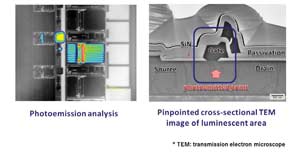
As the company reflects on three decades of service, it is looking forward to two key areas of innovation. The first area is its emphasis on analyzing power semiconductors, which have long been their main service since its founding. For the last 10 years, ITES has been focusing on failure analysis services for compound semiconductor devices, such as silicon carbide (SiC), gallium nitride (GaN), and gallium oxide (Ga2 O3 )—which are recognized as next-generation power semiconductor materials replacing silicon.
The second and more notable area is the company’s advancement in developing cutting-edge inspection systems. These systems are engineered to uncover latent defects in SiC, known as bipolar degradation, before shipment—a serious concern that often slips through the cracks of conventional inspection methods. These defects, if undetected, can expand within the chip over time, leading to increased electrical resistance and, consequently, impacting the device’s reliability.
While ITES’s shift to focus on SiC defect detection has been developed in the recent span of four to five years, it is deeply rooted in the company’s extensive experience with photoluminescence (PL) and electroluminescence (EL) techniques. Being pivotal in the company’s analysis of solar systems, these techniques are now being repurposed and fine-tuned for SiC defect detection, yielding promising results that are set to redefine the landscape of semiconductor technology.
Reducing Time for Failure Analysis and Improving Manufacturing Processes
Failure analysis of power semiconductors consists of three major processes, namely, (1) electrical failure analysis (reproduction of failures that occurred at the customer’s site), (2) identification (narrowing down) of the failure site, and (3) physical analysis of the identified location (cross-sectional observation at the nanoscale; even a deviation of 1μ is not allowed).
Although the analysis methods and techniques required and the equipment used in these three processes are completely different, ITES’s strength lies in its comprehensive capability to perform these processes in a single pass with high accuracy.
Rightly so, in a recent case, ITES pinpointed a minor leakage in a semiconductor device, that seemed to be caused by a foreign material introduced during the formation of the transistor gate, and succeeded in identifying a manufacturing process that needs to be improved. The critical insights enabled the manufacturer to refine their processes and prevent future occurrences of this issue, consequently reducing manufacturing costs.
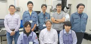
ITES’s Advanced EVC Method for Capturing Critical Latent Defects in SiC Reliability
Since only one failed sample is usually brought into the laboratory, failure such as ‘accidentally cut off the faulty part’ is not acceptable. ITES has the optimum equipment for these three processes and the unique precision processing technology for failed specimens to maximize equipment performance, resulting in an extremely high failure identification rate. This is the reason why they have many repeat customers.
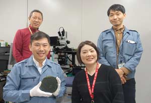
Yasuyuki Igarashi, President and CEO of ITES, emphasizes the value of its precise diagnostics. “With the insights we provide, manufacturers can make quick, specific enhancements to their production line, significantly reducing the time needed to improve the manufacturing process.”
-
With the insights we provide, manufacturers can make quick, specific enhancements to their production line, significantly reducing the time needed to improve the manufacturing process
ITES’s Advanced EVC Method for Capturing Critical Latent Defects in SiC Reliability
ITES’s EVC—Expansion, Visualization, and Contraction—method is a groundbreaking process set to transform semiconductor defect detection and device longevity. This technique replaces the laborious burn-in process traditionally used by device manufacturers, which involves overcurrent stress-testing each individual chip. It is both time-intensive and less efficient, which raises the total cost of production.
In contrast, EVC’s innovative process begins with the application of an ultraviolet (UV) laser system to illuminate the entire wafer.
It is designed to reveal SiC-specific latent defects that would otherwise remain hidden, and cannot be detected by existing inspection systems. Once these defects expand, they become detectable at the wafer level by ITES’s photoluminescence method.
This early detection is crucial. It allows device manufacturers to map out and address potential defects before circuit fabrication. With such defect mapping, manufacturers can avoid incorporating flawed areas into their designs, preemptively eliminating future reliability issues.
Another key process is the heating of the wafers to temperatures around 600 to 800 degrees Celsius for about an hour. The thermal treatment causes the expanded defects to contract and return to their original state. In the current burn-in process, defects remain expanded due to overcurrent stress, so there is a possibility that expanded defects are still present in devices that are shipped as good products. In the EVC method, however, the heating process does not allow expanded defects to be shipped, which can enhance the device’s longevity.
Making a Global Impact with Every Client
The year before last, ITES made headlines at the International Conference on Silicon Carbide and Related Materials (ICSCRM) by unveiling a pioneering system for detecting defects, the EVC method. This global platform drew significant attention from the semiconductor community, leading to a surge of interest from industry leaders worldwide. Following the conference, several major semiconductor manufacturers reached out, entrusting ITES with their wafers to validate this novel defect detection methodology.
The acclaim from these toptier manufacturers has reinforced ITES’s confidence in its methods. To bolster its international reputation further, ITES has been a regular contributor to the ICSCRM and has also presented three technical papers at ICSCRM2023.
On the domestic front, ITES regularly participates in the annual Nanotesting Symposium. Here, ITES gleans insights on new failure analysis technologies and also presents advanced ITES failure analysis methods at its exhibition booth and listens to the reactions of potential customers to remain on the cutting edge of analysis methodologies.
As a total solution service provider to power semiconductor manufacturers, ITES’s strategic vision is set on broadening its horizons. Building on its legacy of providing PC maintenance and repair services since the days of IBM Japan, ITES is poised to introduce specialized repair and maintenance services for power semiconductor testers from FY2024 and propel power semiconductor production into new realms of excellence.
| Share this Article:Tweet
|
Company
ITES
Management
Yasuyuki Igarashi, President and CEO
Description
ITES provides analysis services for semiconductors and other electronic components and materials. It has been analyzing power semiconductors for more than 30 years, and in the past 10 years, it is focusing on failure analysis services for compound semiconductor devices such as SiC, GaN, and Ga2O3, which are considered to be next-generation power semiconductor materials instead of silicon.
This content is copyright protected
However, if you would like to share the information in this article, you may use the link below: