


Thank you for Subscribing to Semiconductor Review Weekly Brief
× 
Semi Conductor Review Weekly Brief
Be first to read the latest tech news, Industry Leader's Insights, and CIO interviews of medium and large enterprises exclusively from Semi Conductor Review
SeeDevice has been recognized by Semiconductor Review Magazine as the exclusive recipient of “Top Quantum-Enhanced CMOS SWIR Image Sensor Manufacturing Solutions 2026,” based on our proprietary methodology, reflecting its position in the industry, and is also named among “Top Semiconductor Manufacturing Services,” reflecting its broader leadership. This profile has been developed by the Semiconductor Review research and editorial team based on insights from an interview with Dr. Hoon Kim, Founder.


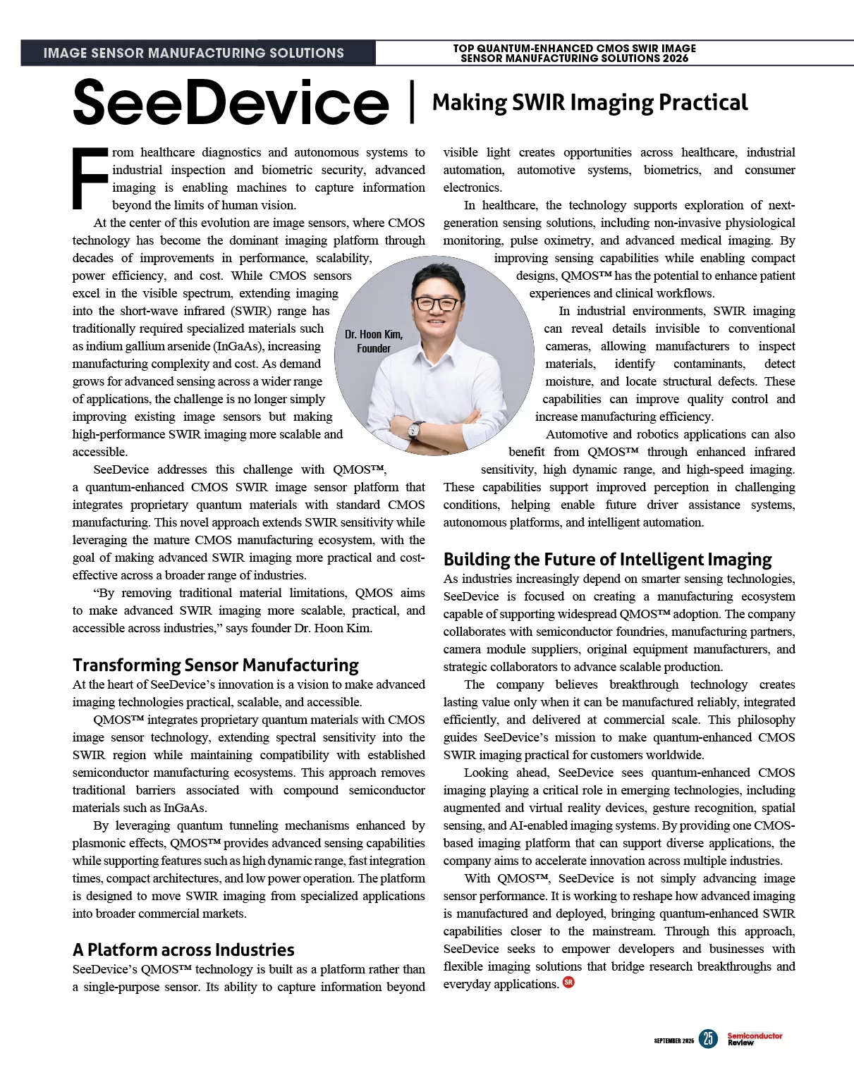
 Dr. Hoon Kim, Founder
At the center of this evolution are image sensors, where CMOS technology has become the dominant imaging platform through decades of improvements in performance, scalability, power efficiency, and cost. While CMOS sensors excel in the visible spectrum, extending imaging into the short-wave infrared (SWIR) range has traditionally required specialized materials such as indium gallium arsenide (InGaAs), increasing manufacturing complexity and cost. As demand grows for advanced sensing across a wider range of applications, the challenge is no longer simply improving existing image sensors but making high-performance SWIR imaging more scalable and accessible.
SeeDevice addresses this challenge with QMOS™, a quantum-enhanced CMOS SWIR image sensor platform that integrates proprietary quantum materials with standard CMOS manufacturing. This novel approach extends SWIR sensitivity while leveraging the mature CMOS manufacturing ecosystem, with the goal of making advanced SWIR imaging more practical and cost-effective across a broader range of industries.
"By removing traditional material limitations, QMOS aims to make advanced SWIR imaging more scalable, practical, and accessible across industries," says founder Dr. Hoon Kim.
Transforming Sensor Manufacturing
At the heart of SeeDevice’s innovation is a vision to make advanced imaging technologies practical, scalable, and accessible.
QMOS™ integrates proprietary quantum materials with CMOS image sensor technology, extending spectral sensitivity into the SWIR region while maintaining compatibility with established semiconductor manufacturing ecosystems. This approach removes traditional barriers associated with compound semiconductor materials such as InGaAs.
By leveraging quantum tunneling mechanisms enhanced by plasmonic effects, QMOS™ provides advanced sensing capabilities while supporting features such as high dynamic range, fast integration times, compact architectures, and low power operation. The platform is designed to move SWIR imaging from specialized applications into broader commercial markets.
A Platform across Industries
SeeDevice’s QMOS™ technology is built as a platform rather than a single-purpose sensor. Its ability to capture information beyond visible light creates opportunities across healthcare, industrial automation, automotive systems, biometrics, and consumer electronics.
In healthcare, the technology supports exploration of next-generation sensing solutions, including non-invasive physiological monitoring, pulse oximetry, and advanced medical imaging. By improving sensing capabilities while enabling compact designs, QMOS™ has the potential to enhance patient experiences and clinical workflows.
-
By removing traditional material limitations, QMOS™ aims to make advanced SWIR imaging more scalable, practical, and accessible across industries.
In industrial environments, SWIR imaging can reveal details invisible to conventional cameras, allowing manufacturers to inspect materials, identify contaminants, detect moisture, and locate structural defects. These capabilities can improve quality control and increase manufacturing efficiency.
Automotive and robotics applications can also benefit from QMOS™ through enhanced infrared sensitivity, high dynamic range, and high-speed imaging. These capabilities support improved perception in challenging conditions, helping enable future driver assistance systems, autonomous platforms, and intelligent automation.
Building the Future of Intelligent Imaging
As industries increasingly depend on smarter sensing technologies, SeeDevice is focused on creating a manufacturing ecosystem capable of supporting widespread QMOS™ adoption. The company collaborates with semiconductor foundries, manufacturing partners, camera module suppliers, original equipment manufacturers, and strategic collaborators to advance scalable production.
The company believes breakthrough technology creates lasting value only when it can be manufactured reliably, integrated efficiently, and delivered at commercial scale. This philosophy guides SeeDevice’s mission to make quantum-enhanced CMOS SWIR imaging practical for customers worldwide.
Looking ahead, SeeDevice sees quantum-enhanced CMOS imaging playing a critical role in emerging technologies, including augmented and virtual reality devices, gesture recognition, spatial sensing, and AI-enabled imaging systems. By providing one CMOS-based imaging platform that can support diverse applications, the company aims to accelerate innovation across multiple industries.
With QMOS™, SeeDevice is not simply advancing image sensor performance. It is working to reshape how advanced imaging is manufactured and deployed, bringing quantum-enhanced SWIR capabilities closer to the mainstream. Through this approach, SeeDevice seeks to empower developers and businesses with flexible imaging solutions that bridge research breakthroughs and everyday applications.
Scaling SWIR through CMOS-Compatible Sensor Manufacturing
SWIR programs often stall between sensor validation and product release. A detector may perform well on a test bench yet impose compound-semiconductor sourcing and nonstandard assembly steps that disrupt the buyer’s established CMOS production path. The resulting cost is not limited to the die. Extra process interfaces affect yield learning, module design, supplier qualification and the time required to move from samples to repeatable volume. That exposure becomes harder to absorb when the target product carries consumer-grade cost limits or compact form-factor requirements. For automotive or consumer deployment, each nonstandard step also raises capital exposure and weakens the volume assumptions behind the product business case.
Procurement teams should examine the proposed manufacturing route before treating spectral performance as the deciding factor. Compatibility with standard CMOS must mean more than attaching an infrared detector to a silicon readout circuit. Buyers need clarity on added materials, wafer-level process steps, foundry portability and the ownership of process control as volumes rise. A design that depends on narrow supplier capacity or difficult heterogeneous integration can preserve the same adoption barrier it was intended to remove.
Performance claims also require application-level interpretation. Broad spectral response has limited purchasing value unless sensitivity remains usable at the wavelengths, exposure times, lighting conditions and temperatures of the intended system. Automotive perception may place greater weight on rapid capture and dynamic range, while industrial inspection depends on contrast through materials or contaminants that visible cameras cannot resolve. Medical sensing introduces a different burden of signal stability and repeatability. The evaluation should connect measured sensor behavior to the actual optical stack, illumination source, detector temperature and readout conditions rather than rely on a single headline specification.
System integration is the next pressure point. Power demand, pixel architecture, package dimensions and calibration requirements shape whether a sensor can enter an existing camera module without forcing a redesign. Firmware and software teams also need predictable output characteristics across temperature and production lots. Early discussions should cover reference designs, interface support, test methods and the division of responsibility between the sensor developer and manufacturing partners. These details determine whether a promising device becomes a manageable component or an extended engineering program.
Commercial readiness is best judged through the path from prototype to supply. Buyers should look for defined foundry relationships, qualified module partners, documented process transfer and inspection controls. Long-term access matters because SWIR programs often serve products with lengthy validation cycles. The stronger supplier is not merely the one with an unusual detection mechanism, but the one that can carry that mechanism into consistent manufacturing while preserving the economics that justified CMOS adoption.
SeeDevice stands out as a premier choice for buyers pursuing quantum-enhanced CMOS SWIR imaging without abandoning the established silicon manufacturing base. Its QMOS platform uses quantum tunneling enhanced by plasmonic effects to extend spectral sensitivity on standard CMOS image sensor technology. The platform also supports high dynamic range, nanosecond-scale integration, compact architectures and low-power system designs. SeeDevice’s fabless model and collaboration with foundries, module suppliers, OEMs and other manufacturing partners directly address the scale-up burden identified earlier. For programs where manufacturability must advance alongside SWIR performance, it offers a focused path worth serious evaluation.
...Read more
Quantum-Enhanced CMOS SWIR Image Sensor Manufacturing Solutions Info
Q1
What Are Quantum-Enhanced CMOS SWIR Image Sensor Manufacturing Solutions?
Quantum-Enhanced CMOS SWIR Image Sensor Manufacturing Solutions extend conventional CMOS imaging into short-wave infrared sensing by using quantum effects within a CMOS architecture. These solutions can combine high sensitivity, fast integration, wide spectral response and scalable manufacturing. The approach is useful where conventional silicon image sensors face limits in detecting wavelengths beyond visible light. It also links advanced sensing performance with a familiar semiconductor manufacturing foundation. These architectures can also reduce reliance on specialized materials and fabrication steps.
Q2
How Does SeeDevice Apply Quantum-Enhanced CMOS SWIR Image Sensor Manufacturing Solutions?
SeeDevice applies Quantum-Enhanced CMOS SWIR Image Sensor Manufacturing Solutions through its QMOS™ technology, which combines quantum tunneling and plasmonics in a CMOS mixed-signal integrated circuit. Its sensors use standard CMOS materials and processes rather than requiring additional materials or manufacturing steps. The company has developed sensors with nanosecond integration time, high sensitivity and a spectral range extending from 200 to 1650 nanometers. These capabilities support imaging across low-light and bright environments.
Q3
Where Are Quantum-Enhanced CMOS SWIR Image Sensor Manufacturing Solutions Used in Practice?
SWIR sensor solutions can support applications that require imaging beyond the visible spectrum or reliable capture under changing light conditions. Documented use areas for SeeDevice's technology include biomedical and biometric systems, automotive applications, security and surveillance, agriculture, consumer devices and machine vision-enabled industrial systems. The combination of rapid integration and broad spectral response can support real-time imaging where moving objects or variable illumination make conventional sensing more difficult.
Q4
What Technical Factors Matter When Evaluating SWIR Image Sensors?
Important factors include spectral range, sensitivity, integration time, dynamic range, noise performance and manufacturing scalability. These measures help determine whether a sensor can meet specific imaging requirements. These solutions should be assessed on how these characteristics work together in the intended imaging environment. A wide spectral range can expand what the sensor detects, while high sensitivity and low noise can improve image data in difficult lighting. Fast integration can also help systems capture moving scenes with less delay.
Q5
How Can Quantum-Enhanced CMOS SWIR Image Sensor Manufacturing Solutions Improve Manufacturing Scalability?
Manufacturing compatibility is an important consideration because SWIR performance has traditionally been associated with specialized materials and processes. CMOS-based SWIR sensing can address this issue when the sensing architecture is designed around established CMOS manufacturing methods. SeeDevice's approach does not require additional materials or processes for its QMOS™ sensors, supporting scalability without disrupting existing CMOS manufacturing processes. This can help connect advanced SWIR capability with more established semiconductor production practices.
Q6
How Can Quantum-Enhanced CMOS SWIR Image Sensor Manufacturing Solutions Support Future Imaging Systems?
These sensor solutions can provide a foundation for imaging systems that need broader spectral access, faster capture and scalable sensor architectures. SeeDevice has also worked on 3D sensing technology for LiDAR and ADAS and developed a non-invasive continuous glucose monitoring device based on its sensing technology. Its broader development work shows how quantum-enabled CMOS sensing can extend beyond conventional imaging into emerging perception and monitoring applications.
| Share this Article:Tweet
|

Company
SeeDevice
Management
Dr. Hoon Kim, Founder
Description
SeeDevice is advancing quantum-enhanced CMOS SWIR imaging with QMOS™, a scalable sensor platform that removes traditional material barriers. By combining quantum technology with CMOS manufacturing, the company enables intelligent imaging solutions across healthcare, automotive, industrial, biometric, and consumer applications.
This content is copyright protected
However, if you would like to share the information in this article, you may use the link below: