
Thank you for Subscribing to Semiconductor Review Weekly Brief
× 
Semi Conductor Review Weekly Brief
Be first to read the latest tech news, Industry Leader's Insights, and CIO interviews of medium and large enterprises exclusively from Semi Conductor Review
Ultratrend Technologies has been recognized by Semiconductor Review Magazine as the exclusive recipient of “Top AlN Single Crystal Wafer Substrate Manufacturer in Asia 2026,” based on our proprietary methodology, reflecting its position in the industry, and is also named among “Top Silicon Wafer Companies In APAC,” reflecting its broader leadership. This profile has been developed by the Semiconductor Review research and editorial team based on insights from an interview with Dr. Liang WU, Founder and CEO.



Ultratrend Technologies
Engineering Bulk AlN for Advanced Semiconductor Platforms

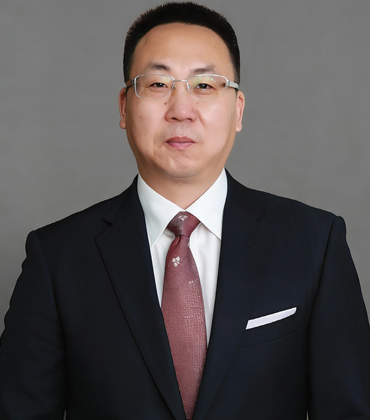 Dr. Liang WU, Founder and CEO
Industrializing bulk aluminum nitride (AlN) single-crystal substrates is one of the most technically demanding challenges in the ultra-wide bandgap (UWBG) semiconductor field. Ultratrend Technologies was founded in 2018 to address this challenge directly, focusing on bringing bulk AlN substrates into real device manufacturing. Headquartered in Hangzhou, the high-tech company was established by senior semiconductor experts who recognized that the future of UWBG electronics depends on substrate materials capable of sustaining extreme electrical, thermal and environmental demands.
Rather than treating AlN as an experimental material, Ultratrend built full fabrication capability from the outset. Its scope spans reactor and hotzone design, modeling and simulation, process optimization, crystal growth, wafering and material characterization. Ultratrend has more than 60 patents applied for and granted, reflecting the depth of proprietary knowledge embedded across its technology stack.
“Bulk AlN growth is not only about producing crystals, but about ensuring they can be consistently adopted in real device manufacturing,” says Dr. Liang Wu, Founder and CEO.
Mastering Bulk AlN Growth
What technical barriers define scalable bulk AlN crystal growth?
 AIN occupies a distinctive position within the UWBG semiconductor family. With an ultra-wide bandgap of 6.2 eV, an exceptionally high critical breakdown field, high thermal conductivity and semi-insulating resistivity, AlN ranks among the top when compared with emerging UWBG materials. These characteristics position it as a foundational substrate for deep-ultraviolet optoelectronics, high-power and high-frequency RF devices and next-generation power electronics.
However, translating these intrinsic advantages into manufacturable substrates remains complex. Bulk AlN growth requires extreme thermal conditions and precise control of carbon and oxygen impurities, which directly impact DUV transparency. Ultratrend’s differentiation lies in how it addresses these challenges at system and process levels.
 The company has strategically adopted tungsten-based growth systems to minimize carbon and oxygen contamination, combined with homoepitaxial growth pathways to maintain crystal integrity. This strategy is supported by a multidisciplinary R&D team spanning materials science, computational modeling and equipment engineering. Ultratrend’s proprietary finite-element simulation platform integrates flow and mass transfer modeling, impurity transport, supersaturation control and three-dimensional stress prediction. These tools are embedded in equipment and process design to shorten development cycles and reduce growth risk.
Multiple generations of fully automated physical vapor transport growth reactors, incorporating tailored hotzones and proprietary processes, have enabled stable material transport and suppression of parasitic nucleation. The outcome is consistent production of high-structural-quality AlN crystals with industry-leading deep-UV transparency.
-
Bulk AlN growth is not only about producing crystals, but about ensuring they can be consistently adopted in real device manufacturing.
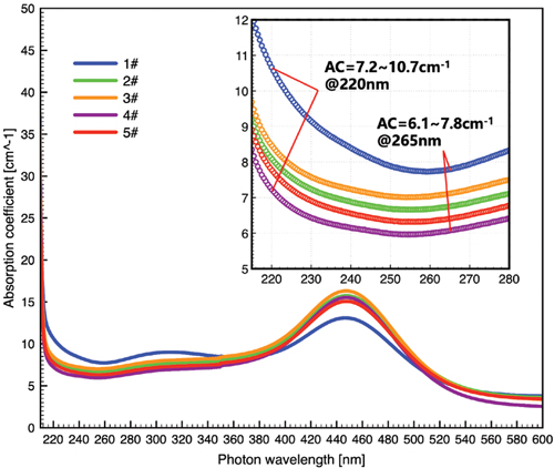
In 2024, Ultratrend introduced 2-inch high-transparency bulk AlN substrates demonstrating absorption coefficients of 7.2–10.7 cm⁻¹ in the 220–240 nm range and as low as 6.1 cm⁻¹ at 265 nm. For the first time, 2-inch PVT-grown AlN substrates achieved DUV transmittance comparable to HVPE-AlN, marking a significant milestone in bulk crystal growth.
Precision at Production Scale
How does Ultratrend ensure quality and reproducibility at scale?
 Ultratrend maintains a comprehensive quality assurance system spanning crystal growth, precision substrate processing and automated inspection. Ultra-high-purity AlN source materials prepared using patented methods are used exclusively, while automated reactors ensure reproducibility across growth runs. Downstream processing includes multi-wire sawing, edge rounding, grinding, polishing and cleaning, delivering epi-ready substrates.
These capabilities translate into measurable outcomes. Ultratrend’s S-grade single-side and double-side polished substrates achieve tight rocking curve values, low total thickness variation and sub-nanometer surface roughness across polar orientations. Reduced dislocation densities enable epitaxial layers with orders-of-magnitude improvement over conventional technologies, supporting high-yield device fabrication.
Beyond standard 2-inch products, Ultratrend supplies non-standard sizes and orientations for R&D applications, manufactured under the same process discipline as volume substrates.
Industrial Scale, Global Reach
What defines Ultratrend’s strategy for global semiconductor adoption?
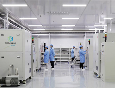 Customers consistently value Ultratrend’s ability to deliver bulk AlN substrates that meet the requirements of scalable manufacturing. Commercial viability, defined by consistent quality, reliable delivery and cost competitiveness, remains central. The company serves more than 160 clients across Asia, Europe and North America, supporting applications ranging from RF and power electronics to deep-ultraviolet optoelectronics. It has also established comprehensive strategic partnerships with renowned downstream device teams, including the Changchun Institute of Optics, Fine Mechanics and Physics (CIOMP), Chinese Academy of Sciences.
To support demand, Ultratrend is executing a phased capacity expansion targeting annual output of 10,000 substrates, alongside plans for a significantly larger production line to enable long-term cost reduction and supply stability.
Strategically, Ultratrend views AlN as the fastest-industrializing UWBG material. Compatibility with existing GaN infrastructure and established PVT scaling models position AlN for accelerated adoption.
Selecting AlN Single-Crystal Substrates for Next-Generation Devices
Ultra-wide bandgap semiconductors are reshaping the technical roadmap for radio frequency electronics, power switching systems and deep-ultraviolet optoelectronics. Among them, aluminum nitride has emerged as a decisive platform material. Its intrinsic properties, including a bandgap of approximately 6.2 eV, a critical breakdown field exceeding 15 MV/cm and thermal conductivity approaching 340 W/m•K, position it at or near the top of major material figures of merit when compared with silicon, silicon carbide, gallium nitride and β-Ga₂O₃ . For executives evaluating substrate supply, the question is no longer theoretical performance but manufacturable consistency and credible scale.
Bulk AlN crystal growth remains technically demanding. Extreme temperatures, tight impurity control and long growth cycles introduce cost and variability risk. Carbon and oxygen contamination, in particular, degrade deep-UV transparency and device performance. A substrate partner must therefore demonstrate mastery over impurity suppression and crystal quality, not only in laboratory demonstrations but across production runs.
The most decisive signal of capability lies in how a manufacturer designs and controls its growth environment. Tungsten-based physical vapor transport systems have gained attention for minimizing carbon and oxygen incorporation. When paired with advanced modeling of mass transfer, impurity transport and stress evolution, such systems enable near-equilibrium growth conditions that translate into improved structural quality. For buyers, evidence of in-house simulation platforms and reactor engineering is a meaningful indicator that process variables are understood rather than approximated.
Wafer processing discipline is equally important. Batchto-batch stability determines yield in downstream epitaxy and device fabrication. High-precision slicing, polishing and cleaning must be integrated with automated inspection so that substrates arrive epi-ready, reducing qualification time. Tight specifications, including rocking curve values at or below 100 arcsec and total thickness variation within single-digit microns, signal that the supplier controls both crystalline perfection and geometry. Low dislocation density is not a marketing metric but a predictor of reduced defect propagation into AlN or AlGaN epitaxial layers, directly affecting device yield.
Executives must also weigh transparency performance in the deep-UV range. Demonstrated absorption coefficients in the Far-UVC band and transmittance comparable to hydride vapor phase epitaxy substrates indicate that bulk PVT-grown wafers are reaching parity in applications once considered out of reach. This has implications for LEDs, lasers and detectors targeting 220–265 nm wavelengths.
Supply assurance cannot be overlooked. Commercial viability depends on consistent quality, reliable delivery and a credible path to cost reduction. The transition from technologypush to demand-pull dynamics in AlN will favor manufacturers that can scale from 2-inch to larger diameters while maintaining material integrity. Clear capacity expansion plans and established collaborations across research and industry ecosystems provide further confidence that production growth will not compromise quality.
Within this landscape, Ultratrend Technologies stands out as a fully integrated AlN single-crystal substrate manufacturer. It operates tungsten-based PVT growth systems supported by proprietary multi-physics simulation tools, enabling control over impurity transport and stress during crystal formation. It delivers 2-inch single-side and double-side polished substrates with documented rocking curve, flatness and surface roughness specifications aligned to advanced RF, power and DUV requirements. It has demonstrated high-transparency bulk substrates in the Far-UVC range and is executing a staged capacity expansion to reach tens of thousands of wafers annually. For executive teams prioritizing material performance, reproducibility and scalable supply, it represents a credible reference point in the AlN substrate market.
...Read more
| Share this Article:Tweet
|
Company
Ultratrend Technologies
Management
Dr. Liang WU, Founder and CEO
Description
Ultratrend Technologies is a Hangzhou-based semiconductor company specializing in bulk AlN single-crystal substrates. With full in-house growth, wafering and quality control capabilities, it delivers high-transparency, high-consistency substrates for RF, power and deep-UV applications at scalable industrial volumes.

This content is copyright protected
However, if you would like to share the information in this article, you may use the link below:
https://www.semiconductorrevieweurope.com/ultratrend-technologies-2026